If you’ve ever worked with printed circuit boards, you know that they can be plagued with a variety of problems. In this blog post, we’ll take a look at some of the most common problems with printed circuit boards and how to solve them.
PCB Design
There are many common problems that can occur during the design of a printed circuit board. Some of the most common problems include:
1. Incorrect trace widths: If the trace widths are not correct, the circuit board will not work properly.
2. Incorrect spacing between traces: If the spacing between traces is not correct, the circuit board will not work properly.
3. Incorrect hole sizes: If the hole sizes are not correct, the circuit board will not work properly.
4. Incorrect solder mask thickness: If the solder mask thickness is not correct, the circuit board will not work properly.
5. Incorrect soldermask registration: If the soldermask registration is not correct, the circuit board will not work properly.
PCB Fabrication
There are many different types of printed circuit board (PCB) fabrication, each with its own set of challenges. The most common problems include incorrect layer stackup, improper etching, and bad soldermask registration.
Layer stackup is perhaps the most important factor in PCB fabrication. If the layers are not properly aligned, the circuit will not work correctly. Etching is another critical step in the process, and if the etching is not done properly, the circuit will be significantly compromised. Finally, soldermask registration is also crucial; if the soldermask does not line up correctly with the underlying circuitry, the circuit will not function properly.
Fortunately, there are ways to avoid these common problems. First, it is important to work with a reputable PCB fabricator that has experience and a proven track record. Second, it is essential to carefully review the design files before sending them to the fabricator. This will ensure that all of the necessary layers are included and that the etching and soldermask registration are correct. Finally, it is always a good idea to test the circuit before putting it into production. By taking these precautions, you can avoid the most common PCB fabrication problems and ensure that your circuit will work correctly.
PCB Assembly
There are a few common problems that can occur during the PCB assembly process. One is misalignment of components, which can happen if the PCB is not properly secured during assembly. This can cause shorts or open circuits. Another problem is incorrect component placement. This can happen if the assembly process is not followed precisely, or if the assembly jig is not correctly aligned. This can cause incorrect connection of traces, vias, and pads. Additionally, poor soldering can result in cold solder joints, which can cause electrical problems. Finally, damaged or missing components can cause the PCB to function improperly.
PCB Rework
There are many potential problems that can occur during the PCB rework process. Some of the most common problems include:
1. Solder Joints – Incorrectly soldered or poorly soldered joints are one of the most common problems that can occur during PCB rework. This can often be due to inexperience or poorly trained technicians.
2. Component Damage – Another common problem that can occur during PCB rework is damage to components. This can often be caused by incorrect soldering techniques or by using too much heat during the rework process.
3. Trace Damage – Another common issue that can occur during PCB rework is trace damage. This can often be caused by incorrect soldering techniques or by using too much heat during the rework process.
4. Warping – Warping is another common problem that can occur during PCB rework. This can often be caused by incorrect soldering techniques or by using too much heat during the rework process.
5. ESD Damage – Electrostatic discharge (ESD) damage is another common problem that can occur during PCB rework. This can often be caused by incorrect soldering techniques or by using too much heat during the rework process.
PCB Reliability
PCB reliability is always a top concern for designers and manufacturers. There are a few common problems that can occur during the PCB design and manufacturing process that can impact reliability.
One common issue is poor solder joint connection. This can happen if the solder joint is not properly cleaned or if the joint is not heated to the correct temperature. Poor solder joint connections can cause electrical shorts or open circuits.
Another common reliability issue is delamination. This can happen when the layers of the PCB are not properly bonded together. Delamination can cause the PCB to crack or break.
Thermal stress can also impact PCB reliability. Thermal stress can occur when the PCB is exposed to extreme temperatures. This can cause the PCB to warp or crack.
Finally, EMI can also impact PCB reliability. EMI is electromagnetic interference that can come from sources such as electric motors or power lines. EMI can cause the PCB to malfunction.
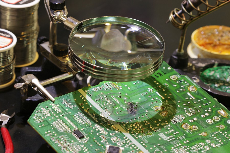
PCB Failure Analysis
PCB failure analysis is the process of determining the cause of a printed circuit board failure. There are many causes of PCB failures, but the most common are electrical shorts, open circuits, and incorrect component values. Other causes of PCB failures include mechanical damage, thermal stress, and chemical contamination. PCB failure analysis can be performed by a variety of methods, but the most common are x-ray inspection, optical inspection, and electron microscopy.
PCB Recycling
PCB recycling is the process of recycling Printed Circuit Boards. Common problems with PCBs include:
-PCBs can be difficult to recycle because they are often mixed with other materials
-There are many different types of PCBs, which makes recycling more difficult
-PCBs often contain hazardous materials, which makes them dangerous to recycle
-PCBs can be difficult to recycle because they often contain valuable metals
-PCBs can be difficult to recycle because they often contain confidential information
PCB Design Tips
There are a few common problems that can occur when designing printed circuit boards. Here are some tips to avoid these problems:
1. Make sure that all traces are the correct width. Traces that are too narrow can cause electrical problems, while those that are too wide can be expensive to manufacture.
2. Pay attention to the spacing between traces. If traces are too close together, they can short circuit, while those that are too far apart can cause signal integrity issues.
3. Make sure that all vias are properly sized. Vias that are too small can cause electrical problems, while those that are too large can be expensive to manufacture.
4. Be careful when using blind or buried vias. These vias can be difficult to manufacture, and they can also cause electrical problems if they are not properly sized.
5. Make sure that all traces are properly routed. Traces that are not routed properly can cause electrical problems, and they can also be difficult to manufacture.
following these tips can help you avoid common problems when designing printed circuit boards.
PCB Design Best Practices
There are four main types of printed circuit board (PCB) design problems:
1. Unrouted or incorrectly routed signal paths
2. Component placement errors
3. Signal integrity issues
4. Power distribution problems
Unrouted or Incorrectly Routed Signal Paths
One of the most common PCB design problems is an unrouted or incorrectly routed signal path. This can happen when a signal trace is not routed properly, or when a via is placed in the wrong location.
Component Placement Errors
Another common PCB design problem is a component placement error. This can happen when a component is not placed in the correct location on the PCB, or when a component is placed too close to another component.
Signal Integrity Issues
A third type of PCB design problem is a signal integrity issue. This can happen when a signal trace is not routed properly, or when a component is placed too close to another component.
Power Distribution Problems The fourth type of PCB design problem is a power distribution problem. This can happen when the power supply is not routed properly, or when a component is placed too close to another component.


More Stories
The Rise to Million-Pound Success: JB Extension’s Journey on TikTok Live!
Top 8 Reasons You Need to Use Executive Search Software
Do You Own a Vehicle With Stop-Start Battery? Can Any Battery Charger be used?